CPU bus circuitry
- smokku
WDC 65C816 CPU has a complex data bus cycle.
It has a 24bit address space, to address 16MB of memory. This is 8 bits more than its predecessor 65C02.
Designers did not want to add 8 more pins to an already large set od CPU pins, so they resorted to a trick.
During first (LOW) half of the PHI2 clock cycle data bus pins (D0-D7) are not used to read/write data,
so these lines are used to provide (A16-A23) signals additionally to A0-A15 provided on dedicated
chip pins. During the second (HIGH) half D0-D7 pins are used to read/write data, so third byte of address
is removed. This requires some kind of latching circuitry, to be able to activate memory chips during
actual data read/write. These is an example, simple circuit diagram in the CPU datasheet.
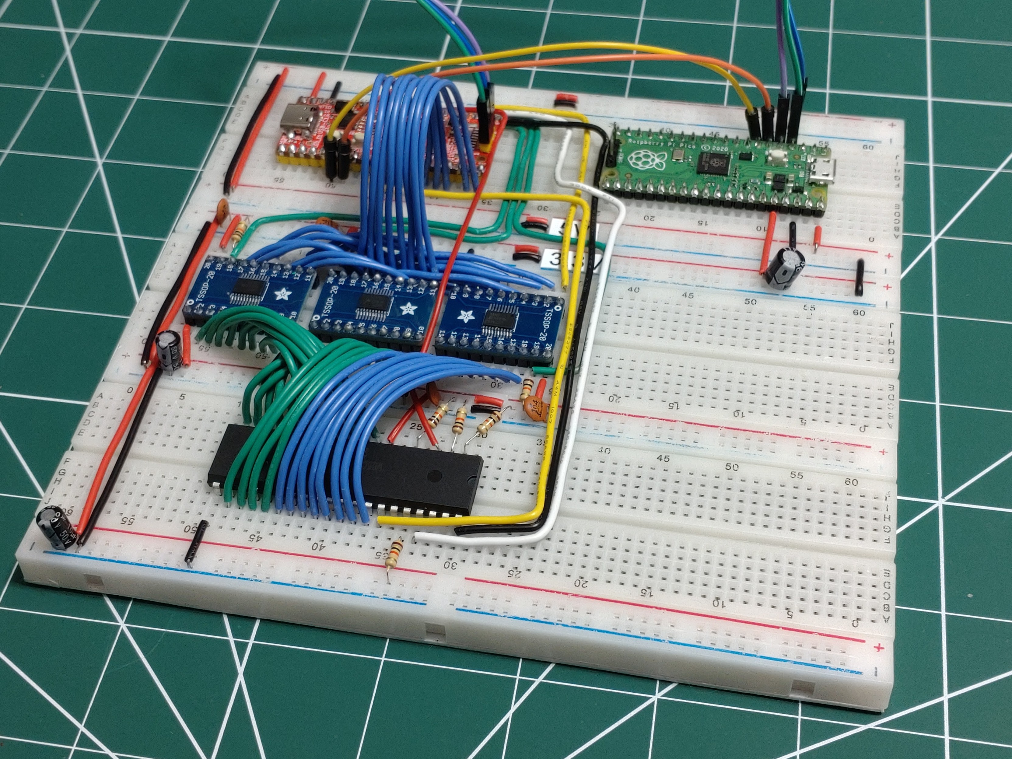
Neo6502 computer is using an interesting design to read/write 65C02 CPU address/data bus.
It has three buffers attached to A0-A15 and D0-D7, used to multiplex 24 CPU lines to only 8 GPIO lines
of RP2040 microcontroller. This design allows handling CPU I/O needs using just 11 pins, instead full 24.
Since 65C816 is using the same set of address/data lines as 65C02, the X65 can use the same circuitry to
handle 65816 CPU just fine, without the need of external latching chips.
The PIO program reads full address from A+D lines while driving PHI2 line low,
switching the buffers CS as fast as possible. Then drives PHI2 high
and switches Data buffer direction to provide CPU with memory-read data. This will allow RP2040
microcontroller to handle full 24bit of address space accesses, emulating RAM, VPU and I/O devices wherever
we want to put them.
Time to wire it up on the breadboard!