Block diagram
- smokku
I’ve finally got around to drawing a block diagram of the X65 DEV-board.
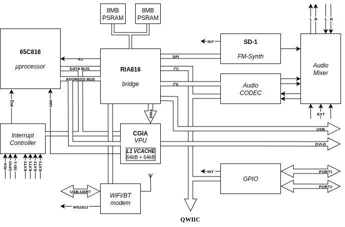
Basically we should think of RIA816 (Raspberry Interface Adapter)
as the north/south-bridge for 65816 CPU and CGIA as a VPU connected via it.
Both were designed in a way, that could be implemented in custom black-box chips.
The fact the current implementation is as microcontroller firmware
is just that - an implementation detail.
CGIA (Color Graphics Interface Adaptor) is designed as an on-bus device, with memory-mapped registers.
It just happens, that current implementation is done using a microcontroller firmware, but that’s just one way.
It could be implemented in FPGA or even in custom ASIC design.