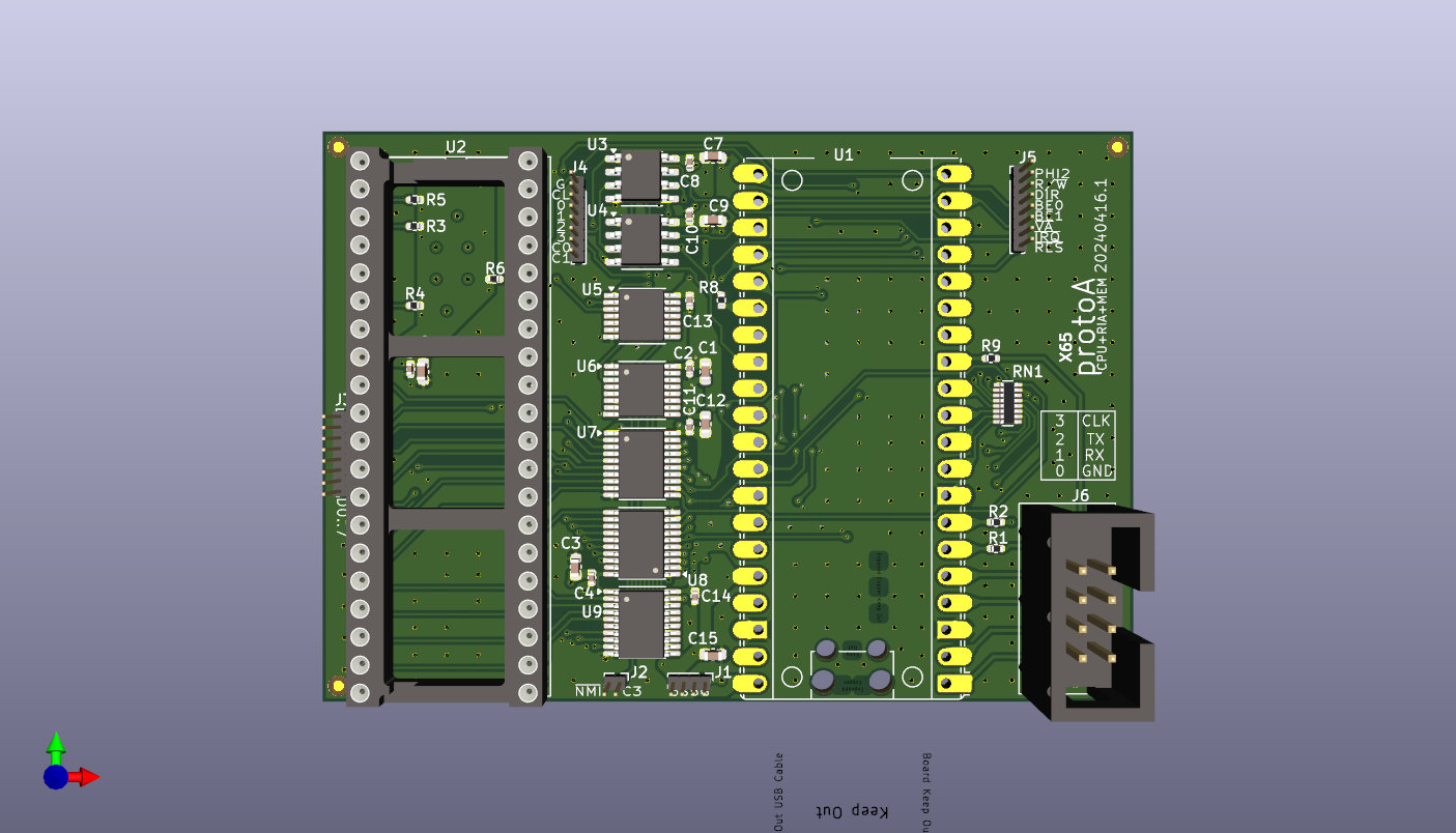
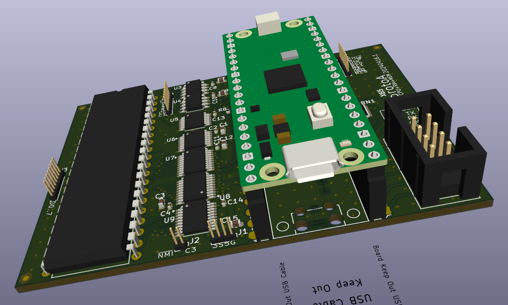
protoA board design
- smokku
The breadboard build reached its frequency limits, so I needed to design a proper
PCB to be able to run RIA firmware full speed.
New QPI PSRAM memory chips will run on 133Mhz. Breadboard is capable of running
a dozen MHz. Even with a /100 PIO clock divider, some memory data patterns being read
from RAM are able to interfere with PIO CLK line and trigger phantom CLK cycles.
This results in dropping nybbles during memory read. A proper, hard-wired PCB is needed.
I’ve spent last few weeks designing a protoA board. This board consists of
CPU + RIA + Memory, connected for current RIA firmware, with external connectors
for upcoming VPU and VIA exposed.
Hopefully this will allow shared full-speed memory access by CPU and VPU.
📒 protoA board schematic PDF
Now, to manufacturing…